Silicon Wafers and Discrete Devices: Precision Dicing
Silicon Wafers and Discrete Devices: Precision Dicing
Silicon is the most common semiconductor material used in wafer dicing. It is a gray brittle material with a diamond cubic structure. Silicon wafers, essential for wafer dicing, are available in sizes up to 12″ in diameter, with 6″ and 8″ being the most common. Typical thicknesses are in the 200 – 800 micron range.
Major Considerations: Key factors affecting wafer dicing include:
Cut quality:
Top-side and back-side chipping
Cracking
Wafer contamination due to ESD issues and poor cleaning
Saw:
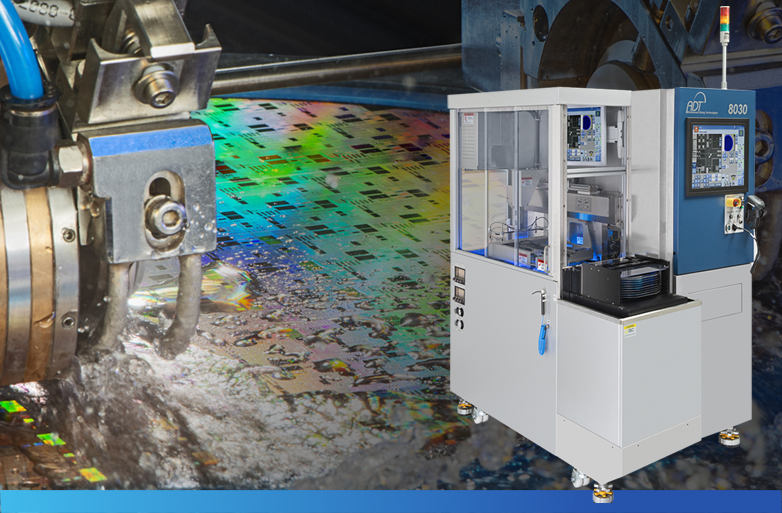
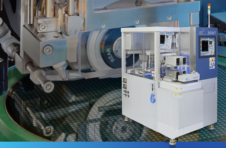
7222, fully automatic wafer dicing saw with WX3 wafer handling system for better throughput and Atomized cleaning or the 7900 Duo automatic Twin spindles for double the throughput