Tech Library / Articles
Singulation of QFN/MLP Packages
30 October, 2012
QFN/MLP substrates behave much differently from most known materials in the microelectronics industry, and therefore present challenges for the dicing process. This paper will cover basic substrate characteristics and various singulation topics.

Package Singulation Processes
31 July, 2006
Dr. Ramon J. Albalak
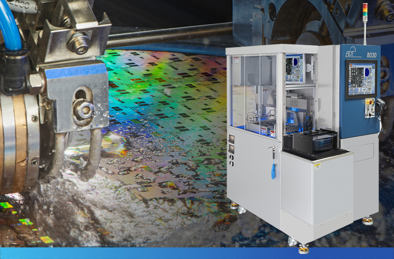
The growing variety and complexity of matrix array packages present a true challenge to many back end processes. The singulation of these arrays into individual packages is an important step in the manufacturing process, and as in many cases, needs to be optimized to minimize the overall cost of package.
Package Singulation Processes (translation into Mandarin Chinese)
31 July, 2006
Dr. Ramon J. Albalak
Challenge to many back end processes. The singulation of these arrays into individual packages is an important step in the manufacturing process, and as in many cases, needs to be optimized to minimize the overall cost of package.
Quality and Reliability Aspects in the Singulation of Complex Wafers Containing Low- k, Copper and TEGs in the Streets
31 July, 2006
Dr. Ramon J. Albalak
A process is presented for the singulation of complex wafers containing low- k, copper and TEGs in the streets.The method is based upon a novel scribing process using a carbon dioxide laser in which a thin top layer of non- silicon elements is removed, followed by a mechanical dicing step that cuts completely through the remaining thickness of the wafer.
The impact of laser scribing on cut quality and resulting die strength is discussed and is compared to that of a traditional two- step dicing.
Dicing Saw Devices
12 July, 2006
Dr. Ramon J. Albalak
SAW (Surface Acoustic Wave) devices are components that make use of the ability of piezoelectric materials to convert acoustic (i.e. mechanical) waves into electromagnetic signals, and vice-versa. By far, the most common SAW devices are SAW Band Pass Filters (SAW BPF) which sort signals by frequency and are used in a large variety of both wired and wireless applications, including cellular phones, cable television equipment, cordless phones, and pagers.
Dicing Saw Devices (translation to Mandarin Chinese)
12 July, 2006
Dr. Ramon J. Albalak
SAW (Surface Acoustic Wave) devices are components that make use of the ability of piezoelectric materials to convert acoustic (i.e. mechanical) waves into electromagnetic signals, and vice-versa. By far, the most common SAW devices are SAW Band Pass Filters (SAW BPF) which sort signals by frequency and are used in a large variety of both wired and wireless applications, including cellular phones, cable television equipment, cordless phones, and pagers.
Dicing Through Hard and Brittle Materials in the Micro Electronic Industry
1 December, 2005
Gideon Levinson
A high percentage of micro electronics dicing applications require dicing completely through the substrate. While partial dicing is relatively easy, dicing through hard and brittle materials creates both mounting and quality problems. The following article discusses various mounting techniques and quality problems related to the dicing process. Recommendations are made to try solve these problems.
Process Optimization of Dicing Microelectronic Substrates
20 October, 2005
Gideon Levinson
The microelectronics industry is constantly seeking improved yields in a wide variety of complicated dicing applications. Continuous efforts are being made to improve both cut quality and through-put. Some new materials have been introduced that require new processes (blades and saws). These trends are accompanied by continuous efforts to further miniaturize die sizes, in order to maximize the number of dies per substrate. To achieve these goals, it is necessary to optimize the dicing process.
Dicing Opto- Electronic Components for the Communication Market
1 December, 2004
Gideon Levinson
The communication market offers an extremely wide array of Opto- Electronic components. This market is still in its growing stage with many new different start- ups introducing new substrate designs and new dicing challenges.
In recent years, new class integrated and tunable optical components have been developed using VLSI compatible technologies and other mature technologies such as MEMS (Micro Electronic Mechanical Systems).
Principles of Dicing
1 February, 2004
Gideon Levinson
Dicing (or diamond-wheel sawing) is used in the microelectronics industry for die separation and also for fine, accurate, partial and cut-through of exotic, very hard and brittle materials. The wide range of materials processed makes it necessary to use different blades. These may be based on hard or soft binders, with various diamond particle sizes.
Considerations for MLF/QFN Substrate Singulation
12 July, 2003
Gideon Levinson
Dicing MLP / QFN substrates behaves very differently from most known materials in the microelectronics industry. This paper will cover the materials structure and behavior, the quality spec that our industry is aspiring toward, the substrate design requirements for optimizing the dicing process and the parameters involved in the dicing process. It will cover in particular the blade options now available and identify opportunities for improvement and optimization.